Table of contents:
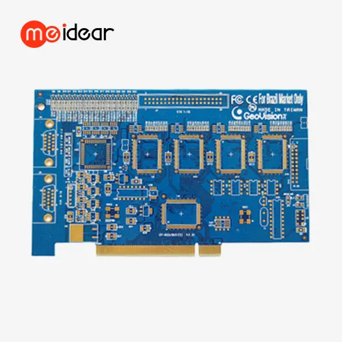
Improving Smartphone Performance with PCB Gold Finger Technology
The Role of Multilayer PCBs in Next-Generation Gaming Consoles
Enhancing Durability of Wearable Tech with Golden Finger PCBs
How Double Layer PCBs Are Shaping the Future of Smart Home Devices
Improving Smartphone Performance with PCB Gold Finger Technology
Smartphones have become an integral part of our daily lives, and their performance hinges on the quality of their internal components. The integration of Double Layer Golden Finger PCBs in smartphone design has led to significant improvements in device speed, reliability, and overall user experience. These advanced PCBs, produced by expert multilayer PCB manufacturers, provide superior conductivity and signal integrity, essential for the high-speed data transfer demands of modern smartphones. The gold-plated connectors ensure consistent performance over time, reducing the risk of connectivity issues that can plague lesser-quality components. As smartphone manufacturers strive to pack more features into slimmer designs, the efficiency and space-saving attributes of these PCBs make them an invaluable asset in the quest for innovation.
The Role of Multilayer PCBs in Next-Generation Gaming Consoles
The gaming industry is constantly pushing technological boundaries, and next-generation consoles are no exception. Multilayer PCBs play a pivotal role in these advanced gaming systems, offering the complexity and performance required to deliver immersive gaming experiences. Multilayer PCB manufacturers are at the forefront of this revolution, producing boards that can handle the intense processing power and heat generation of modern consoles. The implementation of gold finger technology in these PCBs ensures seamless connectivity between components, critical for the split-second responsiveness gamers demand. As gaming consoles evolve into multifunctional entertainment hubs, the versatility and reliability of multilayer PCBs become even more crucial, enabling features like 4K streaming, virtual reality support, and complex AI-driven gameplay.
Enhancing Durability of Wearable Tech with Golden Finger PCBs
Wearable technology faces unique challenges, requiring components that can withstand constant movement, exposure to the elements, and frequent user interaction. Double Layer Golden Finger PCBs are ideally suited for these demanding applications. Their durability and resistance to wear make them perfect for devices like smartwatches, fitness trackers, and augmented reality glasses. The gold-plated connectors maintain their integrity even under frequent use, ensuring reliable data transmission and power delivery. PCB assembly services specializing in wearable tech leverage these advanced boards to create devices that are not only functional but also built to last. As the wearable market expands, the role of robust PCB solutions becomes increasingly vital in developing products that can keep pace with active lifestyles and diverse environmental conditions.
How Double Layer PCBs Are Shaping the Future of Smart Home Devices
The smart home revolution is in full swing, with interconnected devices becoming increasingly prevalent in households worldwide. Double Layer PCBs are at the heart of this transformation, enabling the creation of more intelligent, efficient, and compact smart home devices. These PCBs, crafted by skilled multilayer PCB manufacturers, provide the perfect balance of functionality and size for products like smart thermostats, security cameras, and voice-controlled assistants. The precision and reliability of gold finger technology ensure consistent performance, crucial for devices that are expected to operate seamlessly around the clock. As the Internet of Things (IoT) ecosystem grows, PCB assembly solutions tailored for smart home applications are becoming essential, facilitating the development of devices that can communicate effectively and operate efficiently within the connected home environment.
The use of Double Layer Golden Finger PCBs in consumer electronics highlights their versatility and importance in modern technology. From boosting smartphone performance to powering gaming consoles, improving wearable tech, and enabling smart home innovations, these PCBs drive progress across many applications. As consumer demands grow, multilayer PCB manufacturers and specialized assembly services will remain key to delivering innovative, reliable, and high-performance devices. With golden finger PCB technology, the future of consumer electronics promises more advanced, durable, and efficient products that enhance daily life.

No comments:
Post a Comment